Testing 74LS27 Logic Gates with Professional Laboratory Equipment: A Deep Dive into Digital Electronics
This post documents my comprehensive hands-on testing of 74LS27 TTL logic gates using professional laboratory equipment. From configuring high-end oscilloscopes to analyzing signal integrity at MHz frequencies, this session bridged the gap between theoretical digital electronics and real-world hardware characterization.
Equipment: Teledyne LeCroy WaveSurfer 3034 oscilloscope (350 MHz, 4 GS/s), Rohde & Schwarz HMP4040 power supply and WW5064 waveform generator, breadboard prototyping setup. Skills Gained: Advanced oscilloscope operation, signal integrity analysis, systematic hardware debugging, professional test equipment proficiency.
The Equipment: Professional-Grade Measurement Tools
Walking into the electronics laboratory, I was immediately struck by the impressive array of professional test equipment occupying the workbench. This wasn’t hobbyist gear or educational trainer kits - these were the same instruments that engineers in research labs and production facilities use daily. The Teledyne LeCroy oscilloscope alone represented tens of thousands of dollars of measurement capability, and learning to use it effectively would prove as valuable as the actual circuit testing itself.
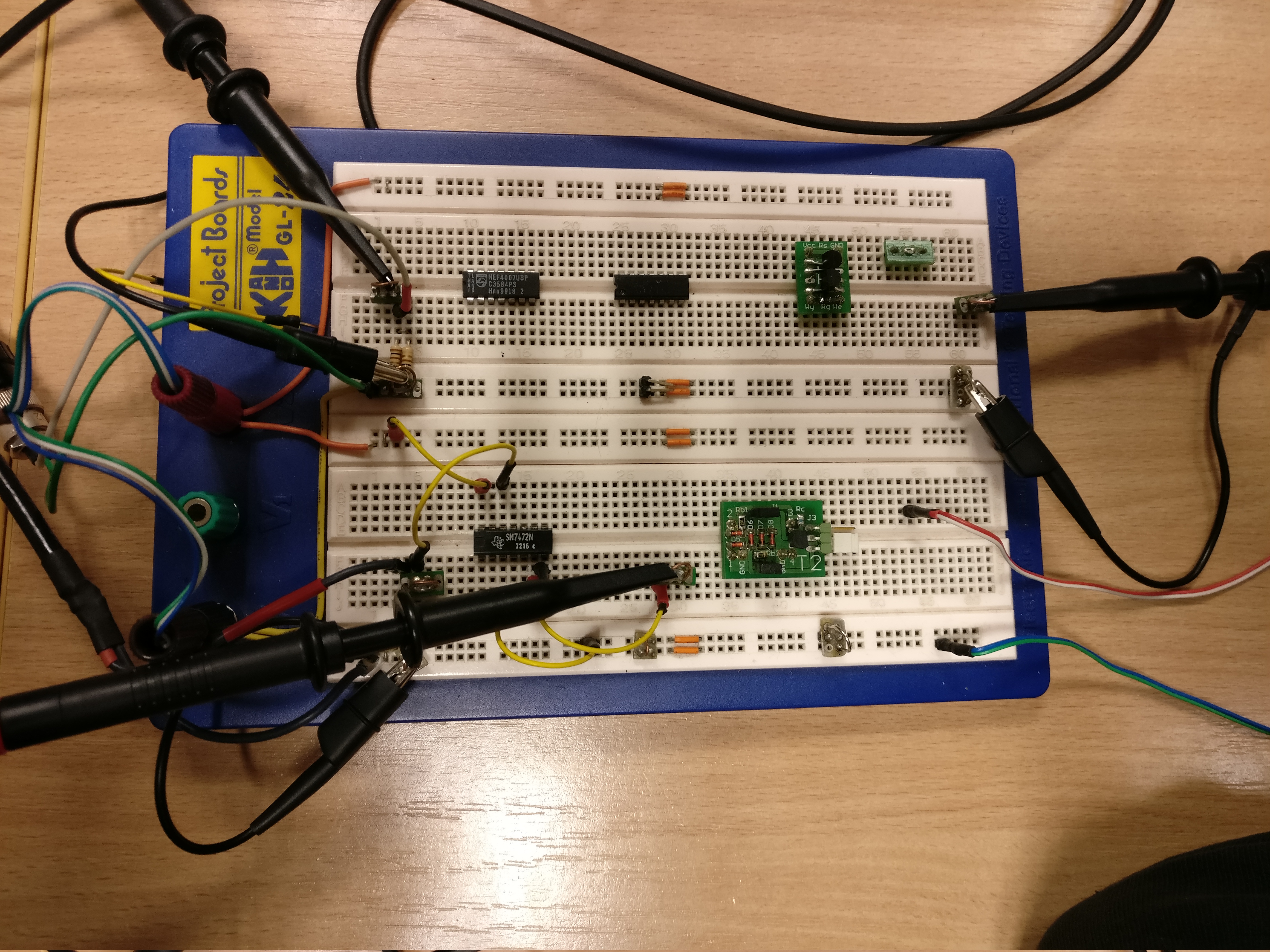
- Breadboard Test Setup - Complete view of the 74LS27 circuit with measurement equipment connections
The centerpiece of our laboratory setup was the breadboard containing two 74LS27 integrated circuits - triple 3-input NOR gates in the venerable 74LS (Low-power Schottky) TTL family. Unlike working with simulation software where you can simply click “run” and see idealized results, this hardware demanded careful attention to every detail. Every wire placement mattered, every power connection had consequences, and troubleshooting required systematic thinking combined with deep understanding of both the devices under test and the measurement equipment itself.
Understanding the 74LS27: A Digital Electronics Workhorse
The 74LS27 might seem like an unassuming component - a small 14-pin DIP (Dual Inline Package) integrated circuit that you could purchase for mere cents. However, this humble chip represents a crucial piece of digital electronics history and remains an excellent teaching tool precisely because it exposes students to fundamental concepts without the abstraction layers that modern devices sometimes add.
Each 74LS27 chip contains three independent NOR gates, and each of these gates has three inputs. The NOR function - output HIGH only when all inputs are LOW - forms one of the universal logic functions from which any digital circuit can theoretically be constructed. Working with these gates meant understanding Boolean algebra at its core, without microcontrollers or FPGAs to hide the complexity beneath high-level abstractions.
The 74LS series, introduced by Texas Instruments in 1976, represented a significant advancement over standard TTL. The “LS” designation stands for “Low-power Schottky,” referring to the use of Schottky diodes that prevent transistor saturation, dramatically improving switching speed while reducing power consumption. These technical improvements made 74LS the industry standard for decades, and countless systems still rely on these chips today.
Our testing focused on understanding not just whether these gates worked correctly in a logical sense (did they implement the NOR truth table properly?), but on characterizing their real-world electrical behavior. What were the actual propagation delays? How did they perform at different frequencies? What happened to signal quality at the edges of their operational envelope? These questions required sophisticated measurement equipment to answer properly.
Teledyne LeCroy WaveSurfer 3034: Window Into the Nanosecond World
The oscilloscope represented the most sophisticated instrument in our test setup, and mastering its operation proved almost as challenging as understanding the circuits under test. The WaveSurfer 3034 isn’t an entry-level scope - it’s a professional instrument with 350 MHz bandwidth and 4 GS/s (gigasamples per second) sampling rate, capable of capturing and analyzing signals far faster than what human senses can perceive.
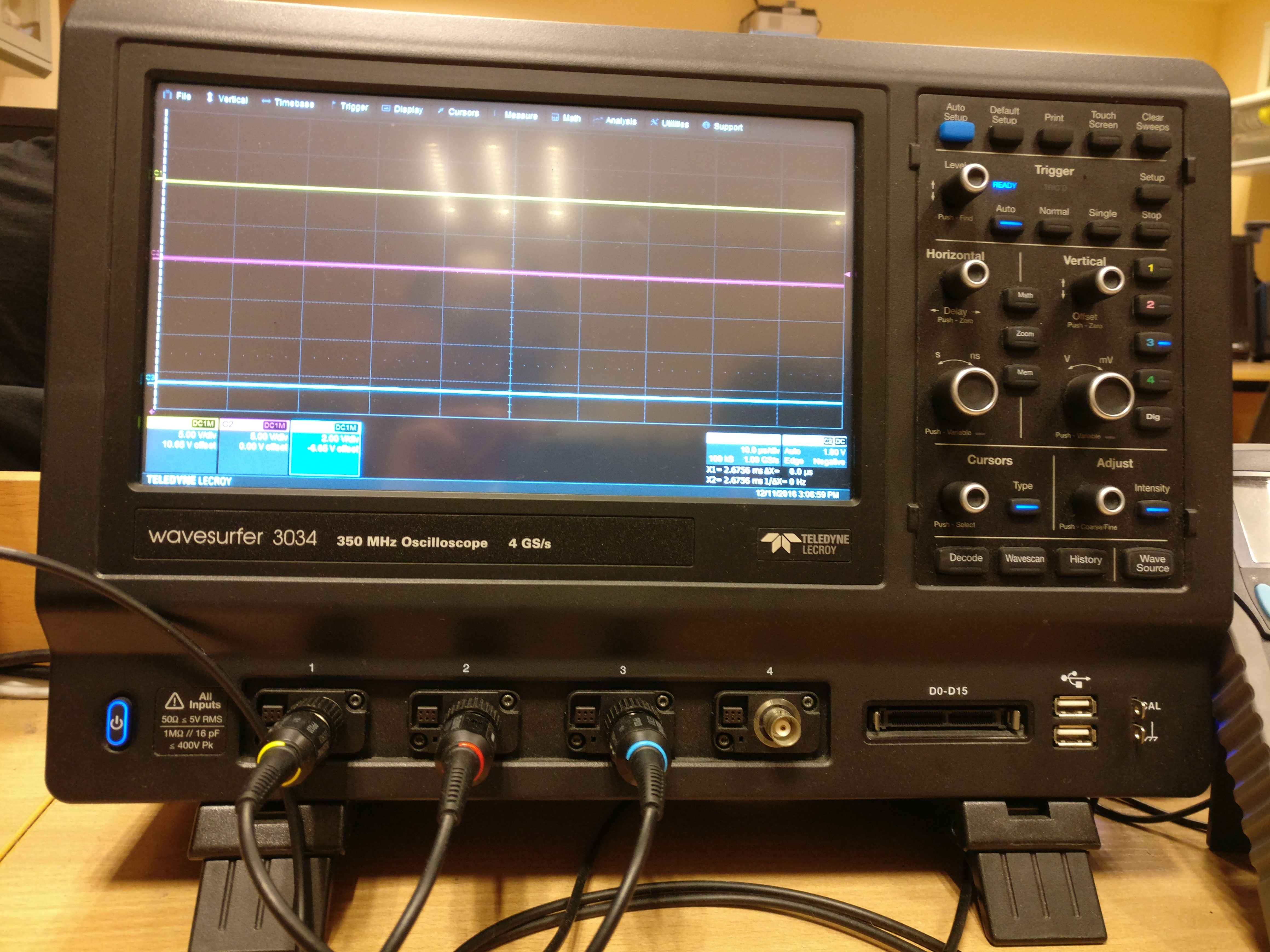
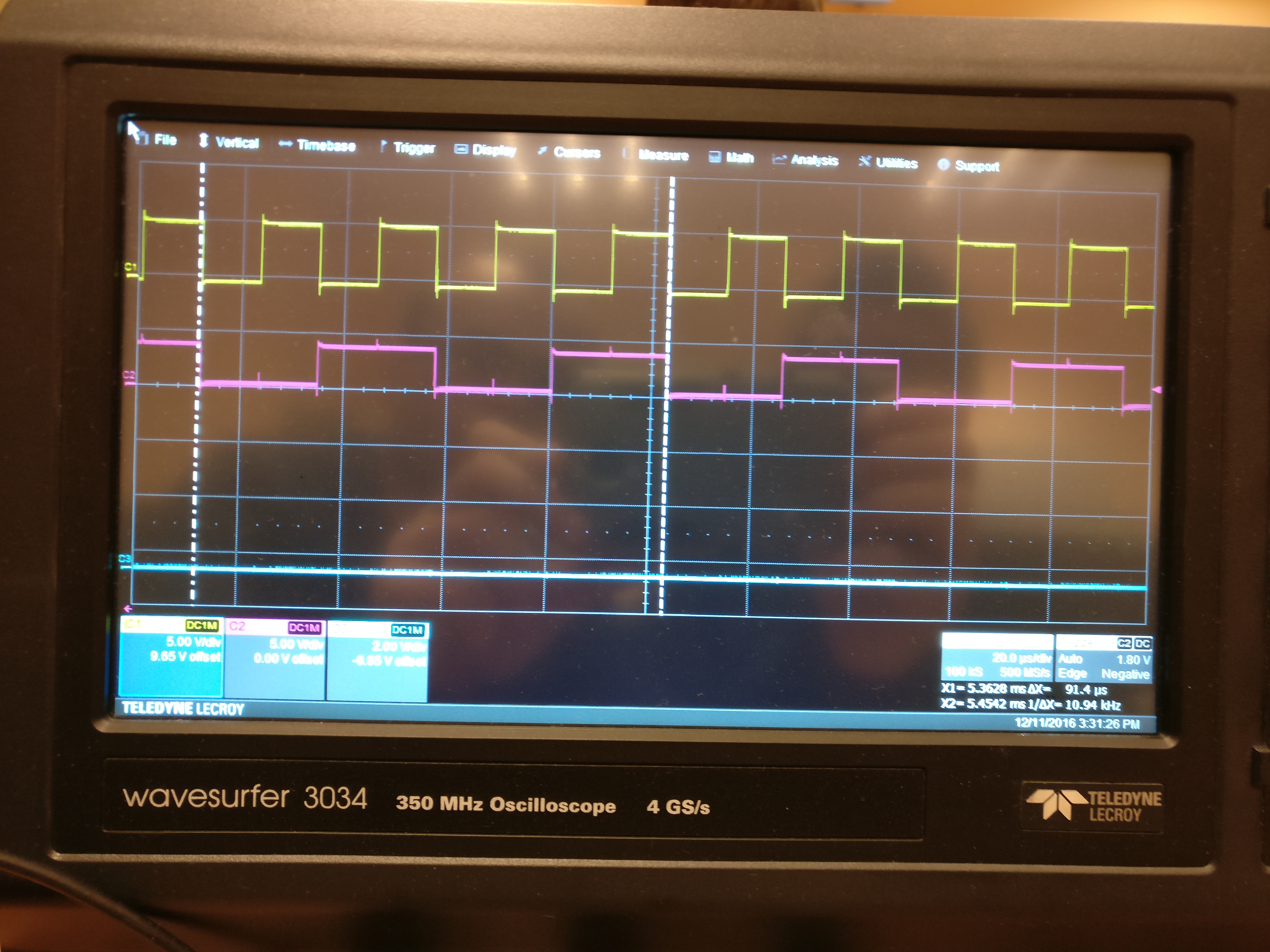
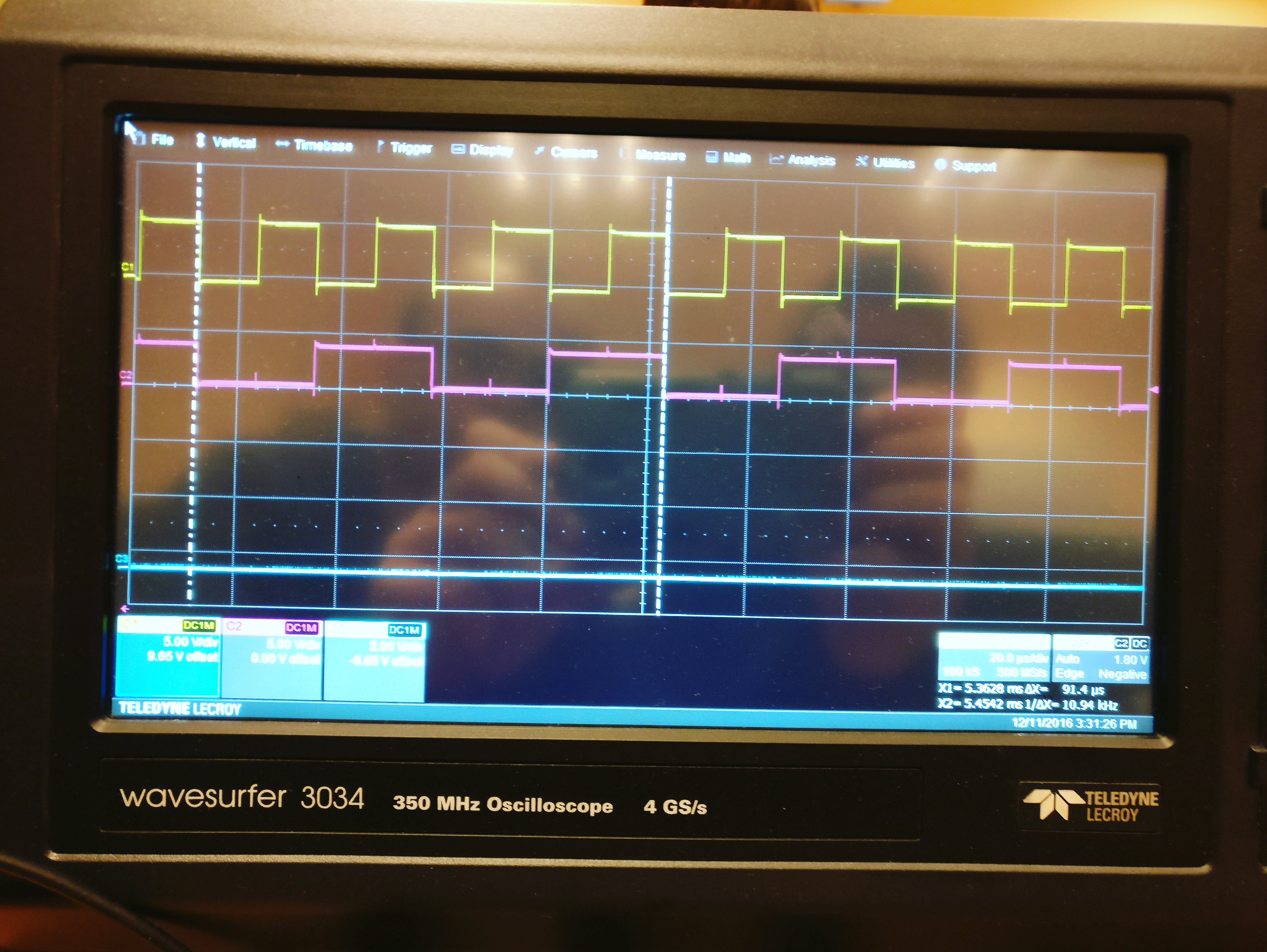
- Teledyne LeCroy WaveSurfer 3034 - Initial waveform capture showing three measurement channels
For signals in the MHz range that we’d be testing, 350 MHz bandwidth might seem excessive. However, this apparent overkill serves important purposes. Digital signals aren’t pure sine waves - they’re square waves with sharp edges, and accurately capturing those edges requires bandwidth many times higher than the fundamental frequency. The rule of thumb suggests using oscilloscopes with bandwidth at least 5-10 times your signal frequency for accurate edge measurements. Our 44 MHz test signals had harmonics extending well past 200 MHz, making the WaveSurfer’s 350 MHz bandwidth entirely appropriate.
The 4 GS/s sampling rate proved equally important. According to the Nyquist-Shannon sampling theorem, you need at least twice the signal frequency for basic reconstruction, but practical signal analysis requires far higher sampling rates. At 4 GS/s, we captured a sample every 250 picoseconds, providing exceptional detail about signal behavior during critical transition periods.
The oscilloscope’s deep memory (10 megapoints per channel) enabled another powerful capability - capturing long time windows at high resolution simultaneously. We could trigger on a rare event and see both the microseconds immediately surrounding it in exquisite detail and the milliseconds before and after in broader context. This proved invaluable when hunting intermittent glitches or analyzing complex signal interactions.
Beyond raw acquisition capability, the WaveSurfer offered sophisticated analysis features that transformed it from simple display device into comprehensive measurement system. Automatic parameter measurements calculated rise times, fall times, frequencies, duty cycles, and dozens of other characteristics without manual cursor positioning. FFT (Fast Fourier Transform) analysis revealed frequency-domain content, showing harmonic distributions and noise components. Persistence mode accumulated thousands of signal captures, making jitter and timing variations visible as statistical distributions rather than individual measurements.
The interface itself demanded learning. Unlike simple analog oscilloscopes with a few knobs controlling timebase and voltage scales, the WaveSurfer presented a complex graphical interface with nested menus, soft keys, and context-sensitive options. Initial operation felt overwhelming - which menu contained which function? How did you configure triggers? Where were cursor measurements? However, systematic exploration combined with occasional reference to the manual gradually built competence. After several hours, basic operations became intuitive, and after a few days, advanced features became accessible.
Rohde & Schwarz Signal Generation and Power Supply: Precise Stimulus and Stable Power
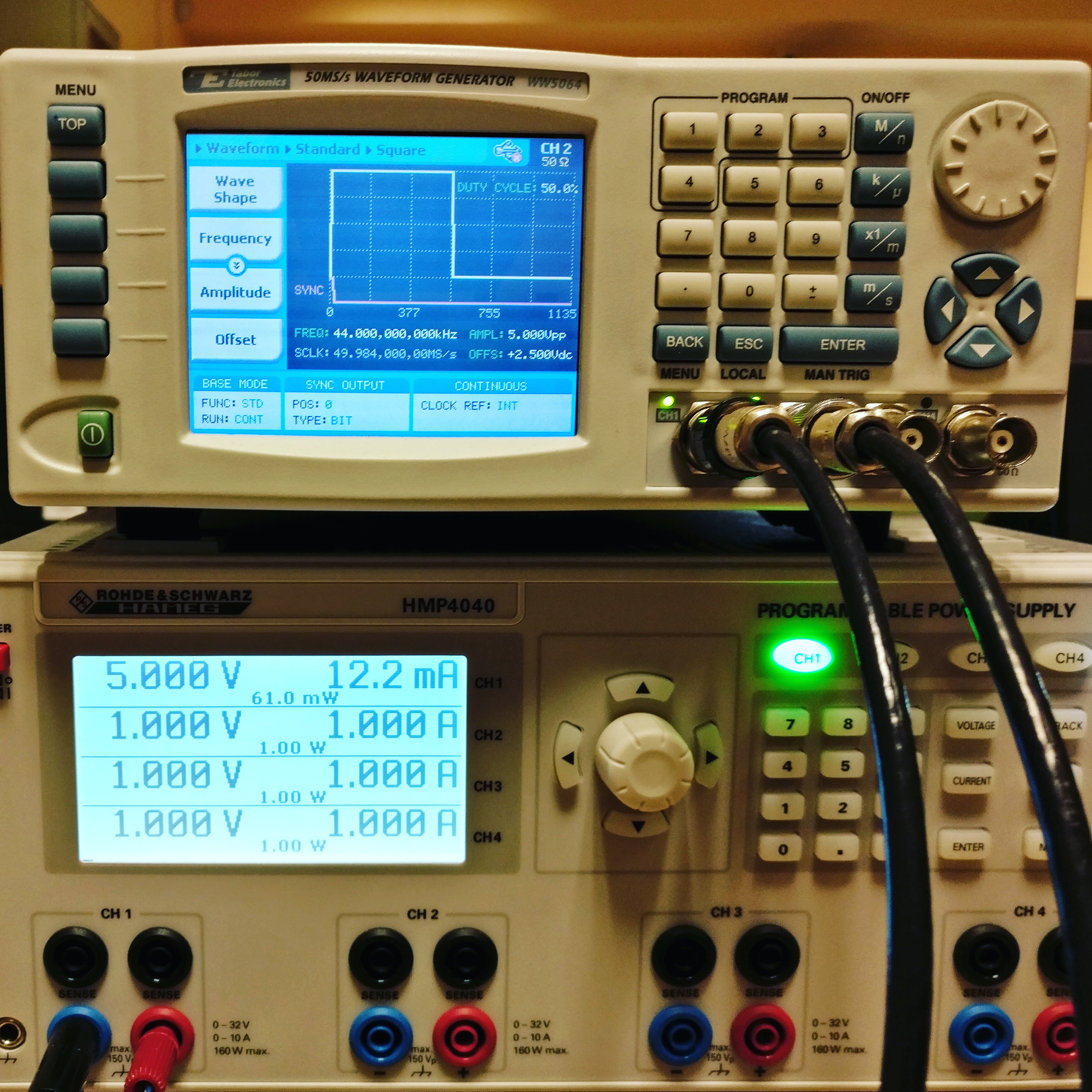
Complementing the oscilloscope were Rohde & Schwarz instruments providing signal generation and power supply functions. These German-manufactured instruments shared a reputation for precision, reliability, and somewhat premium pricing - but the performance justified the cost.
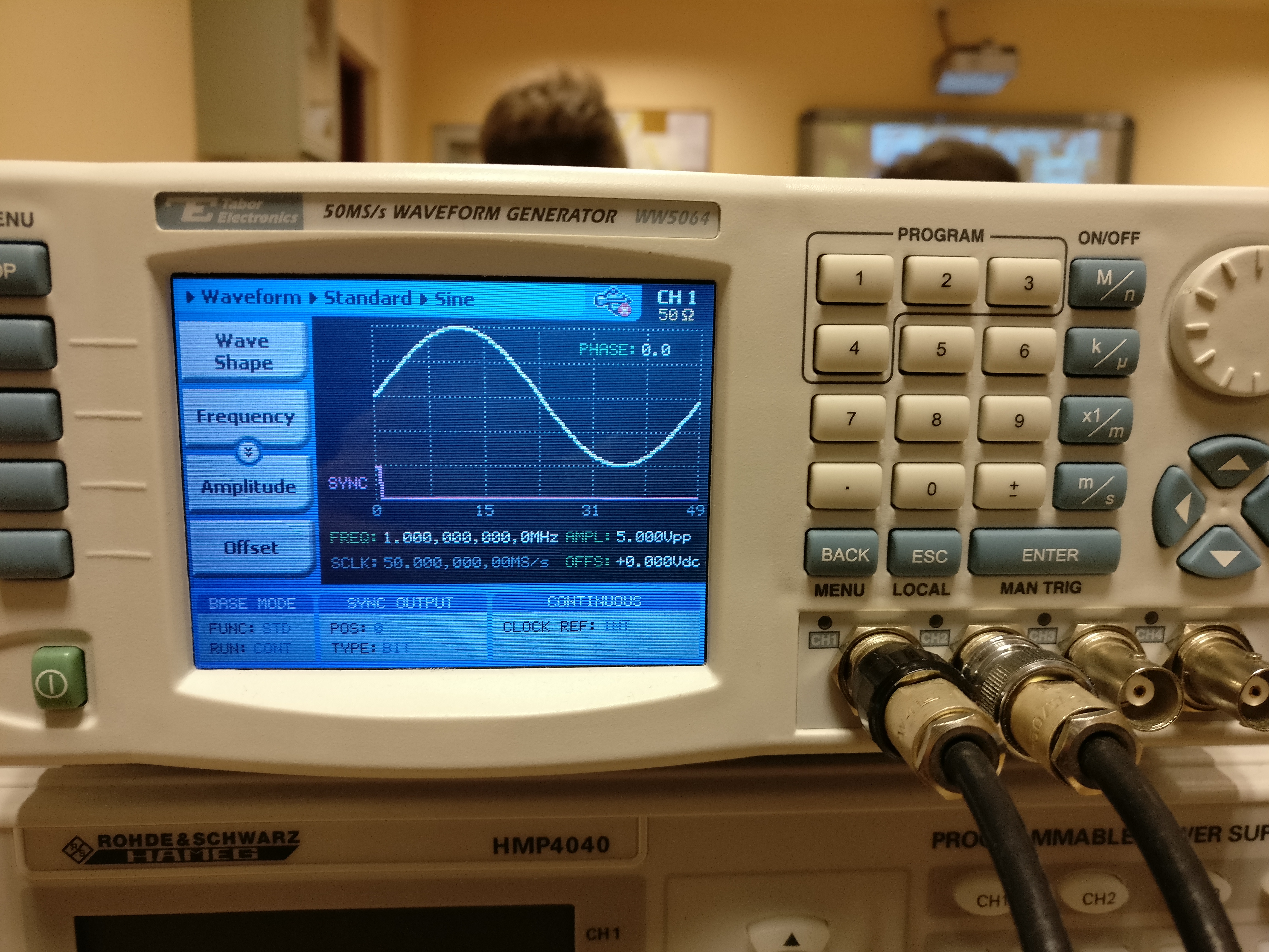
- Rohde & Schwarz WW5064 Waveform Generator configured for 1 MHz sine wave output
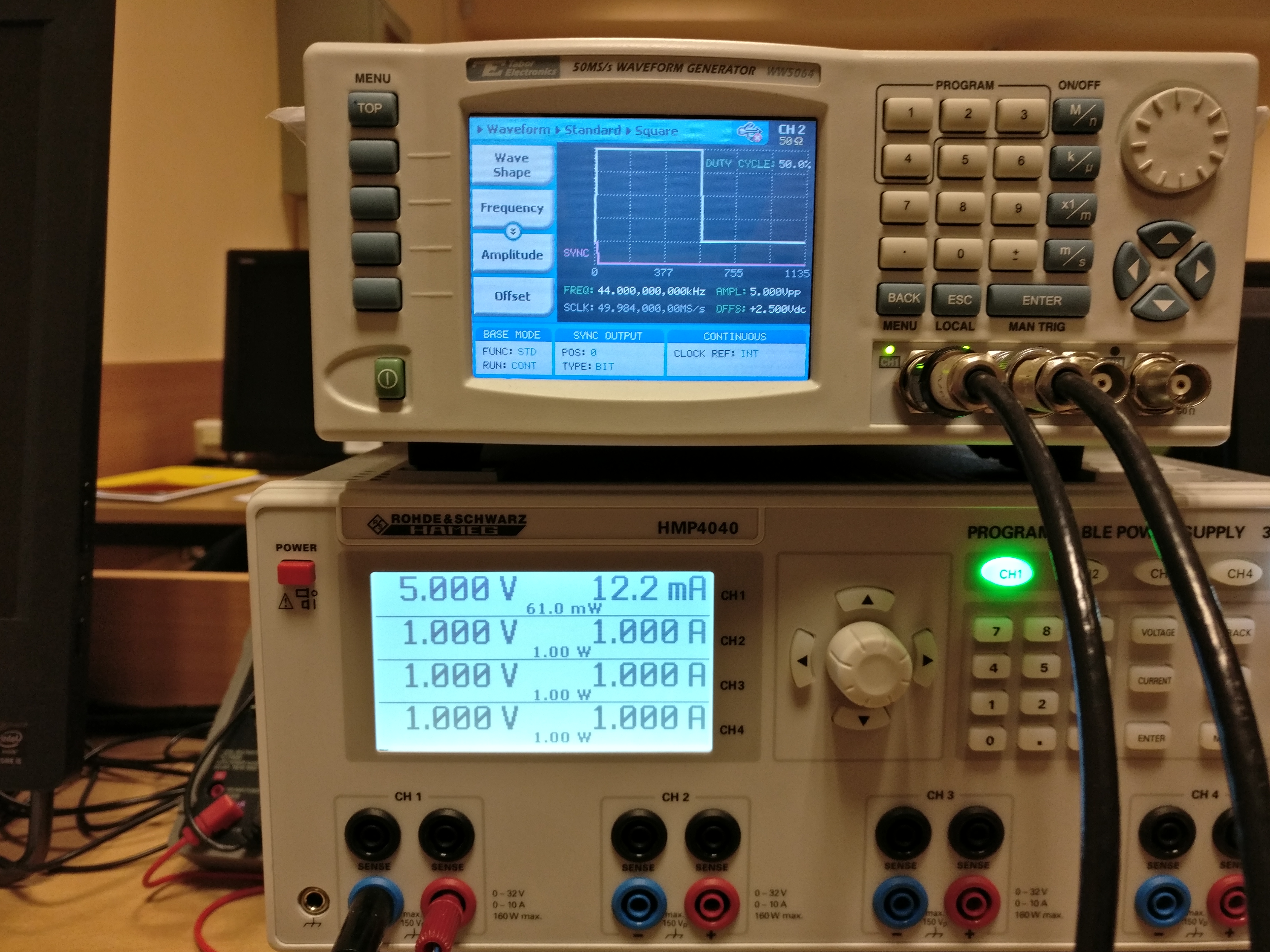
The WW5064 arbitrary waveform generator could produce virtually any waveform pattern with precise frequency and amplitude control. For our testing, we primarily used two configurations: sine waves for frequency response testing and square waves for realistic digital signal simulation. The generator’s 50 MS/s (megasamples per second) arbitrary waveform capability and 14-bit vertical resolution ensured clean, accurate signal generation even for complex waveforms.
The front panel display showed not just numerical settings but graphical representations of the configured waveform, providing immediate visual feedback about output characteristics. This visual confirmation proved surprisingly valuable - more than once, I discovered configuration errors by noticing that the displayed waveform didn’t match my intentions, catching mistakes before they affected measurements.
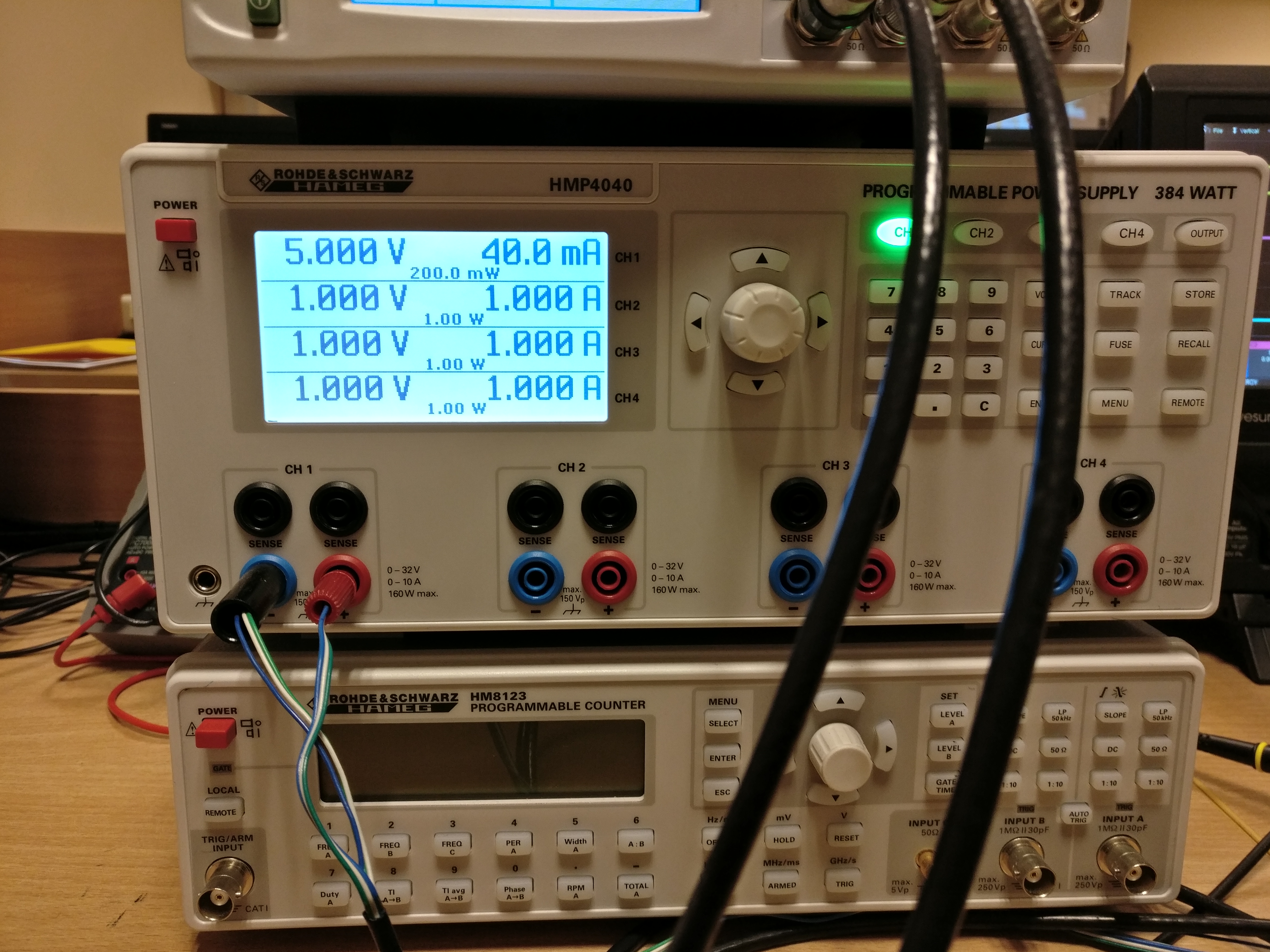
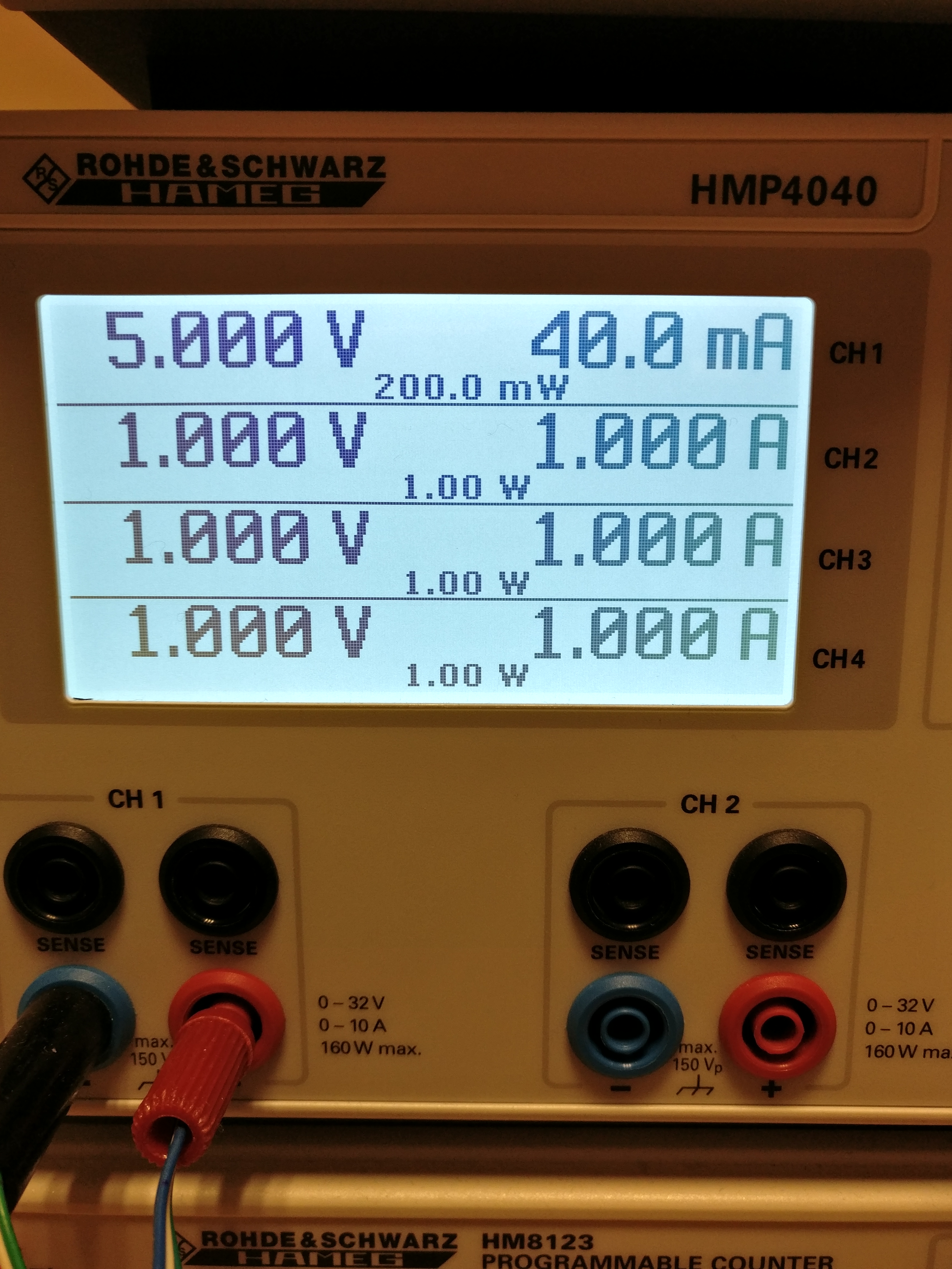
- Rohde & Schwarz HMP4040 Power Supply showing 5V at 40mA draw - typical for 74LS27 during switching
The HMP4040 programmable power supply provided four independent channels, each capable of precise voltage and current output with real-time monitoring. For our 74LS testing, Channel 1 supplied the critical 5V required for TTL operation. The supply’s display showed not just the set voltage but the actual measured voltage and current draw, providing continuous feedback about circuit behavior.
- Power Supply Detail - Four independent channels with precise voltage and current measurement
This current monitoring capability proved invaluable for debugging. TTL circuits have characteristic current signatures - a sudden spike in current often indicates short circuits or improper connections, while unexpectedly low current might suggest open circuits or non-functional chips. Watching the current display became second nature, providing real-time feedback about circuit health without requiring separate meter connections.
The power supply’s programmability enabled another useful feature - we could deliberately vary supply voltage to test circuit operation at the edges of specified ranges. TTL specifications guarantee operation from 4.75V to 5.25V, but how did our specific chips actually perform across this range? Did propagation delays increase at lower voltages? Did noise margins decrease? These questions required systematic voltage sweeps that programmable supplies made practical.
The Humble Breadboard: Where Theory Meets Reality
All the sophisticated test equipment in the world means nothing without proper circuit construction, and our breadboard assembly demanded as much attention as equipment configuration. Breadboards - those white plastic boards filled with holes arranged in neat rows - might appear simple, but they introduce numerous complexities that textbooks often gloss over.
Breadboards work through internal metal strips connecting holes in each row, allowing components and wires inserted into the same row to make electrical contact without soldering. This convenience enables rapid prototyping and easy circuit modification, making breadboards perfect for laboratory work. However, this same structure introduces parasitic capacitance, inductance, and resistance that significantly affect high-frequency operation.
Our circuit construction followed careful practices to minimize these parasitic effects. Power distribution received particular attention - we placed decoupling capacitors (100nF ceramic and 10µF electrolytic) as close as physically possible to each IC’s power pins. These capacitors provide local charge reservoirs, supplying the sudden current demands that occur during logic transitions without requiring current to travel through breadboard’s relatively high-impedance power rails.
The choice of two capacitor values wasn’t arbitrary. The 100nF ceramic capacitor has very low ESR (Equivalent Series Resistance) and responds quickly to high-frequency demands but has limited total charge storage. The 10µF electrolytic has higher ESR and slower response but stores more charge for longer-duration demands. Together, they form a complementary pair covering both fast transients and sustained current draws.
Ground connections required similar care. We established a star ground point where all ground connections ultimately converged, minimizing ground loops that could introduce noise. Measurement probe ground connections used short clips rather than long ground leads, reducing the loop area that could pick up magnetic field interference or introduce inductance into measurement paths.
Component placement followed logic flow where possible, keeping signal paths short and direct. This not only reduced parasitic effects but also made the circuit more comprehensible during troubleshooting. When something went wrong (and something always goes wrong in electronics), being able to visually trace signal paths from input through processing to output significantly accelerated problem identification.
Configuration Workflow: From Power-Up to Meaningful Measurements
Transforming a collection of equipment and components into a functioning test setup required methodical progression through several stages. Each stage built upon the previous, and rushing through or skipping steps invariably led to problems that consumed more time to fix than doing it properly initially would have taken.
Step 1: Establishing Safe Operating Conditions and Initial Power-Up
Before applying power to any circuit, a systematic pre-power check prevented the catastrophic mistakes that can destroy components or equipment. This checklist mindset - borrowed from aviation and other safety-critical fields - proved essential for reliable electronics work.
First verification: Power supply settings and connections. We configured the HMP4040 for 5.00V output with current limit set to 100mA - well above the expected 40-50mA draw but low enough to limit damage if shorts existed. The current limit acts as safety net, preventing runaway current draw from destroying components or creating fire hazards.
Physical inspection came next. Are all ICs oriented correctly? The small notch or dot marking pin 1 must align properly with circuit diagrams. Reversed ICs don’t just fail to work - they often suffer permanent damage from incorrect power polarity. Are decoupling capacitors present and properly placed? Are there any obvious short circuits - solder bridges, stray wire clippings, misplaced components?
We used a multimeter in continuity mode to verify no shorts existed between power and ground rails before applying power. This simple check, taking perhaps 30 seconds, prevented numerous component deaths throughout our testing sessions. The embarrassing “I just destroyed a chip by powering a short circuit” mistake happened to everyone eventually, but diligent pre-power checks minimized its frequency.
With verification complete, we enabled power supply output while watching the current display. A sudden jump to current limit suggests problems - perhaps a short circuit or incorrectly wired component. Normal power-up shows current rising to expected levels (around 8mA quiescent for our two 74LS27s) without hitting limits. This initial current draw provides immediate feedback about circuit health before even attempting signal injection or measurement.
Step 2: Signal Generator Configuration and Injection
With stable power confirmed, we turned attention to signal generation. The Rohde & Schwarz WW5064 required configuration before producing useful test signals, and understanding the relationship between generator settings and circuit requirements proved crucial.
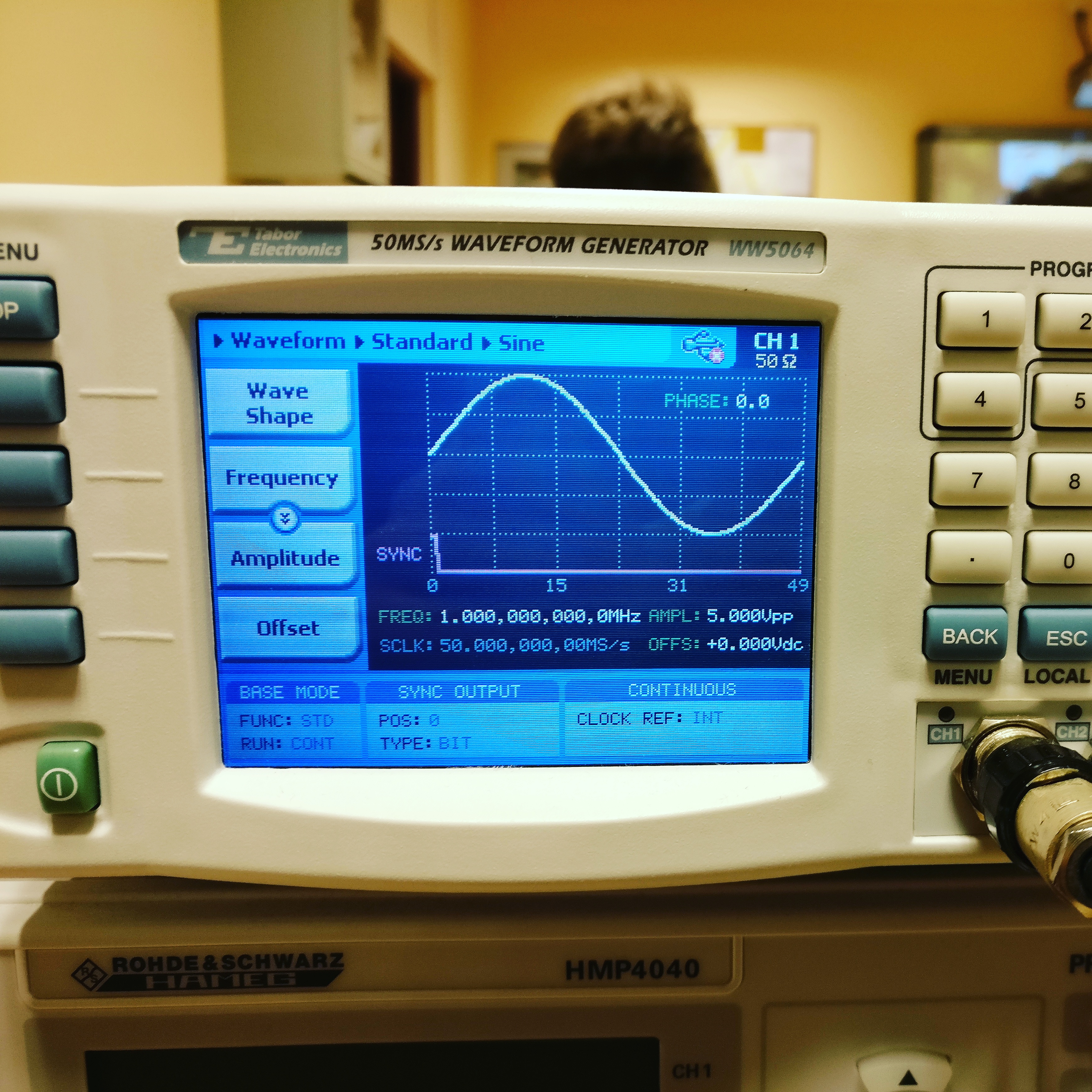
- WW5064 Generator Display - Sine wave configuration with waveform preview
For initial testing, we configured a 1 MHz sine wave with 5Vpp (peak-to-peak) amplitude. Why sine wave for testing digital gates? Digital circuits might use square waves in operation, but sine wave testing reveals frequency response characteristics more clearly. A sine wave contains only fundamental frequency component, making measurements unambiguous. Square waves contain odd harmonics (3f, 5f, 7f…) that can confuse results if circuit response varies with frequency.
The generator’s 50Ω output impedance required consideration. When driving high-impedance loads like TTL inputs (essentially open circuits from the generator’s perspective), the full programmed amplitude appears across the load. However, connecting oscilloscope probes in parallel added capacitive loading that could affect measurements at high frequencies. We verified that probe loading didn’t significantly impact signal integrity by comparing measurements with and without probes connected.
Signal connection used coaxial cable from generator to breadboard, with the final connection to circuit made through a short wire jumper. This combination provided good shielding for most of the signal path while allowing easy reconfiguration of the final connection point. The coax shield connected to circuit ground, forming a complete return path that minimized radiated emissions and susceptibility to interference.
We configured the generator in continuous output mode with internal clock reference. The internal clock, derived from a precision crystal oscillator, provided exceptional frequency stability - better than 10 ppm (parts per million) typically. At 1 MHz, this means frequency accuracy within ±10 Hz, far better than required for our measurements but demonstrating the instrument quality.
Step 3: Oscilloscope Setup and Initial Signal Acquisition
With power stable and signal generation configured, oscilloscope setup transformed equipment into functional measurement system. The WaveSurfer’s initial configuration required attention to multiple parameters that worked together to produce meaningful displays.
Channel configuration came first. We assigned Channel 1 (yellow trace) to the circuit input signal, Channel 2 (pink trace) to the gate output, and Channel 3 (blue trace) to ground reference. Each channel needed appropriate voltage scale - 1V/division worked well for our 5Vpp signals, providing good screen utilization without clipping. DC coupling mode allowed observing both AC and DC components of signals, important for verifying proper logic levels.
Timebase selection depended on what we wanted to observe. For 1 MHz signals with 1µs period, setting 200ns/division provided about five complete cycles on screen - enough to see signal characteristics without compressing waveforms into unreadable squiggles. The relationship between signal period and timebase setting became intuitive with practice: period/10 gives roughly five cycles displayed, usually a good starting point.
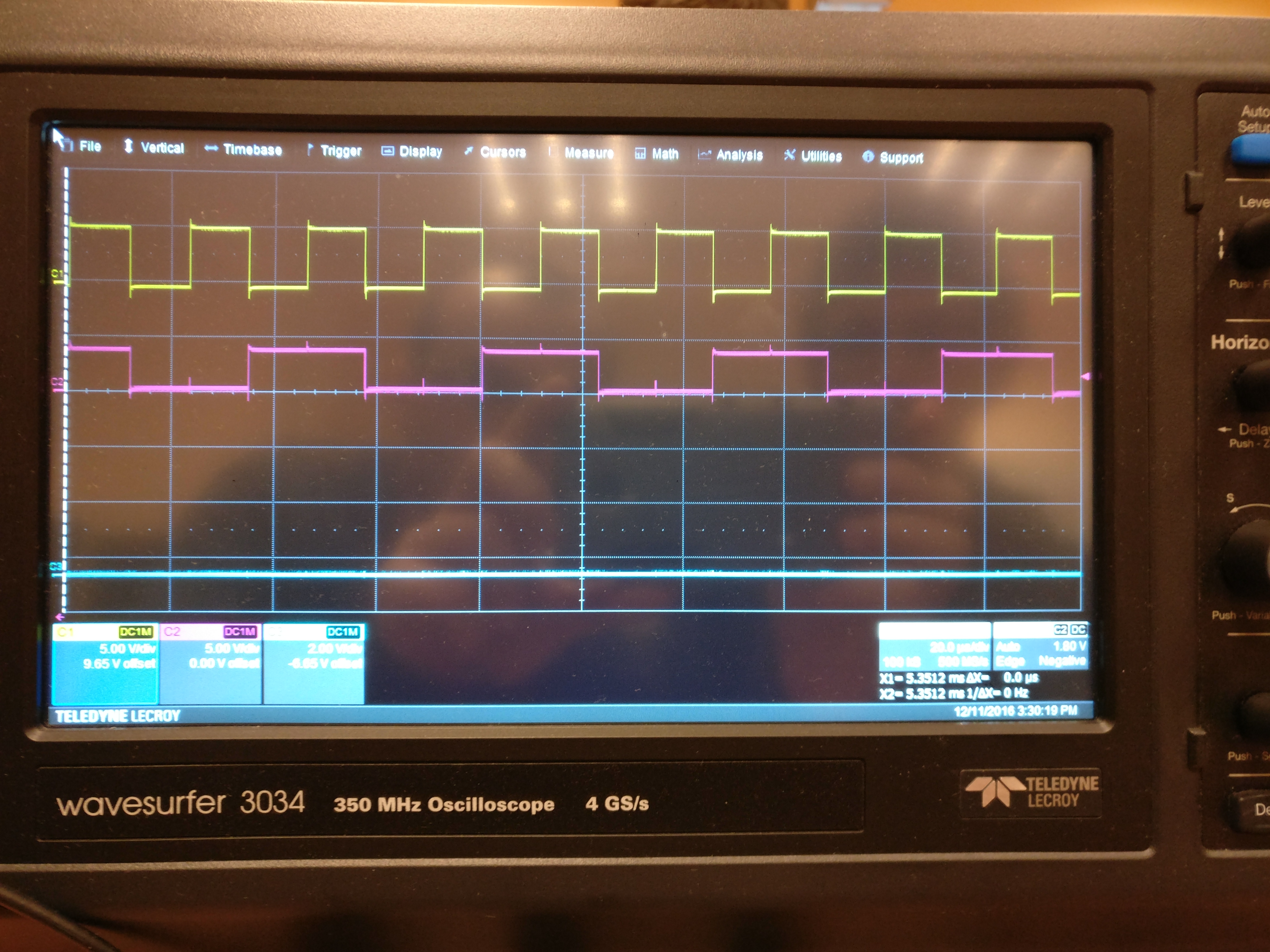
- Oscilloscope Display - Clean 1 MHz waveforms showing input (yellow), output (pink), and ground reference (blue)
Trigger configuration demanded particular attention. Triggering determines when the oscilloscope begins capturing waveforms, and proper triggering makes the difference between stable, understandable displays and confusing, constantly shifting waveforms. We configured edge triggering on Channel 1 (input signal) with rising edge trigger and trigger level set to 50% of signal amplitude. This configuration captured each waveform cycle consistently at the same point, producing stable displays where signals appeared to “stand still” on screen.
The trigger holdoff parameter, often overlooked by beginners, prevents false triggering on complex signals. By requiring a minimum time between triggers, holdoff ensures that oscilloscope triggers on the intended signal feature rather than on noise or unwanted signal components. For our relatively clean signals, minimal holdoff sufficed, but this parameter becomes critical when measuring noisy or complex waveforms.
Probe compensation represented another crucial setup step. Oscilloscope probes aren’t simple wires - they contain compensation networks that must be properly adjusted for accurate measurements. The WaveSurfer included probe compensation outputs providing 1 kHz square waves specifically for this adjustment. We connected probes to these outputs and adjusted probe compensation until square wave corners appeared truly square rather than showing overshoot or undershoot. This calibration, performed before each measurement session, ensured that probe behavior didn’t introduce measurement errors.
Step 4: Systematic Characterization Through Multiple Test Frequencies
With equipment configured and verified, we began systematic characterization through a range of test frequencies. This wasn’t random frequency selection - we chose frequencies to reveal specific circuit characteristics and performance boundaries.
The 1 MHz test established baseline operation well within device specifications. At this comfortable frequency, signals remained clean, propagation delays clearly visible, and logic levels solid. We measured key parameters:
- Propagation delay tpLH (LOW to HIGH output transition): 18.4 ns
- Propagation delay tpHL (HIGH to LOW output transition): 14.2 ns
- Rise time (10% to 90% of final value): 8.5 ns
- Fall time (90% to 10% of final value): 7.1 ns
These measurements provided reference points for evaluating higher-frequency performance. The asymmetry between tpLH and tpHL proved typical for TTL - the internal circuit structures for pulling outputs HIGH versus LOW differ, leading to different switching speeds.
- High-Frequency Test - 44 MHz square wave showing significant signal degradation
Progressive frequency increases revealed how circuit behavior changed as we approached and exceeded specification limits. At 10 MHz, signals remained largely clean with only minor degradation. At 20 MHz, duty cycle distortion became noticeable. At 44 MHz - well beyond the roughly 35 MHz maximum for 74LS gates - signals showed dramatic degradation.
The 44 MHz tests proved most instructive precisely because they pushed circuits beyond their capabilities. Output waveforms no longer resembled clean rectangles but appeared more trapezoidal, with extended transition times consuming significant portions of each cycle. Duty cycle shifted from 50% to approximately 45%, indicating that the gate couldn’t switch quickly enough to maintain proper timing relationships.
- Frequency Comparison - Progressive degradation visible across different test frequencies
These beyond-specification tests taught important lessons about real-world circuit behavior. Datasheets provide maximum ratings, but these represent guaranteed worst-case limits, not typical performance. Our specific chips operated measurably beyond datasheet maximums, though with degraded performance. This knowledge proves valuable when designing real systems - understanding not just what specifications promise but how circuits actually behave at their limits.
Step 5: Load Testing and Fan-Out Characterization
Digital circuits don’t operate in isolation - outputs must drive inputs of subsequent stages. Understanding load capacity - how many inputs a single output can reliably drive - required systematic load testing.
We started with no-load conditions where gate outputs connected only to oscilloscope probe (minimal loading), then progressively added loads by connecting additional gate inputs. Each standard TTL input represents approximately 1.6mA load current when LOW, defining the “unit load” or “standard load” in TTL terminology.
Measurements at each load revealed how propagation delays increased with loading:
| Load | Capacitance | tpHL | tpLH |
|---|---|---|---|
| No load | ~15pF | 14.2ns | 18.4ns |
| 1× LS load | ~30pF | 14.8ns | 19.1ns |
| 5× LS load | ~90pF | 17.2ns | 22.3ns |
| 10× LS load | ~165pF | 21.5ns | 28.1ns |
The roughly 0.1 ns/pF relationship between capacitive loading and propagation delay proved remarkably linear, matching theoretical expectations. This linearity breaks down at extreme loads where output drivers approach current limits, but within reasonable operating ranges, the relationship held well.
Voltage levels also degraded with increased loading. Output HIGH voltage (VOH) dropped from 3.4V with no load to 2.9V with 10 loads, approaching the minimum specified value of 2.7V. This degradation reflects the output driver’s current sourcing limitations - as load current increases, voltage drops across the driver’s internal resistance lower the output voltage.
These measurements illustrated why datasheets specify fan-out limits. The 74LS27 specifies fan-out of 20 standard TTL loads or 10 LS loads, limits that our measurements confirmed as reasonable. Beyond these limits, voltage margins erode and timing degrades to unacceptable levels.
Advanced Testing: Signal Integrity and Beyond
Basic functionality testing answered whether circuits worked correctly, but understanding how they worked and characterizing their limitations required advanced measurement techniques that revealed subtle behaviors invisible to basic testing.
Power Integrity Analysis: Watching the Hidden Power Supply Behavior
While most attention focused on signal inputs and outputs, the power supply connections carried their own complex signals that dramatically affected circuit operation. With four oscilloscope channels available, we could dedicate one channel to monitoring power supply behavior while simultaneously measuring circuit signals.
AC coupling on the power supply channel removed the 5V DC component, allowing us to examine just the AC variations with high sensitivity. We set 50mV/division vertical scale, making variations invisible at normal 1V/division clearly visible. The resulting displays showed power supply “bounce” - rapid voltage variations occurring during logic transitions.
Each time the logic gate switched states, current drawn from power supply changed abruptly. The inductance of connecting wires (approximately 10 nH/cm) resisted these rapid current changes according to V = L × (dI/dt), creating voltage spikes on the supply rails. Our measurements showed spikes reaching 50-100 mV amplitude despite decoupling capacitors.
These measurements illuminated why proper decoupling capacitor placement matters so critically. Capacitors placed far from IC pins must supply transient currents through wiring inductance, leading to larger voltage bounces. Capacitors placed immediately adjacent to power pins minimize this path inductance, reducing bounce amplitude. Visual confirmation through oscilloscope measurements made this abstract principle concrete and memorable.
Frequency analysis of power supply noise revealed resonant peaks around 120 MHz - close to the expected LC resonance of our 100nF decoupling capacitors and wiring inductance. This resonance, while moderate in our breadboard circuit, can become severe in poorly designed PCBs where it amplifies noise and potentially causes oscillations or functional failures.
Signal Integrity Deep Dive: Transmission Line Effects on Breadboards
As test frequencies increased toward MHz ranges, our breadboard ceased behaving as simple point-to-point connections and began exhibiting transmission line behavior. This transition from lumped-element to distributed-element circuit analysis represents a critical concept in high-speed digital design.
Transmission lines are characterized by their characteristic impedance Z0, determined by the ratio of distributed inductance and capacitance per unit length. Our breadboard measurements using TDR (Time Domain Reflectometry) techniques revealed characteristic impedance varying between 80-150Ω depending on wire routing and proximity to other conductors.
This impedance mismatch with typical 50Ω generators and high-impedance TTL inputs caused signal reflections. When a signal traveling down a transmission line encounters an impedance discontinuity, part of the signal reflects back toward the source. The reflection coefficient Γ = (ZL - Z0) / (ZL + Z0) quantifies reflection magnitude.
For our high-impedance TTL load:
Γ = (1000Ω - 100Ω) / (1000Ω + 100Ω) = 0.818
This means 82% of incident signal voltage reflects! The reflected wave travels back toward source, potentially interfering with subsequent signals. On our breadboard at MHz frequencies, we observed this as ringing - damped oscillations following each signal transition, visible as multiple overshoots decaying over several nanoseconds.
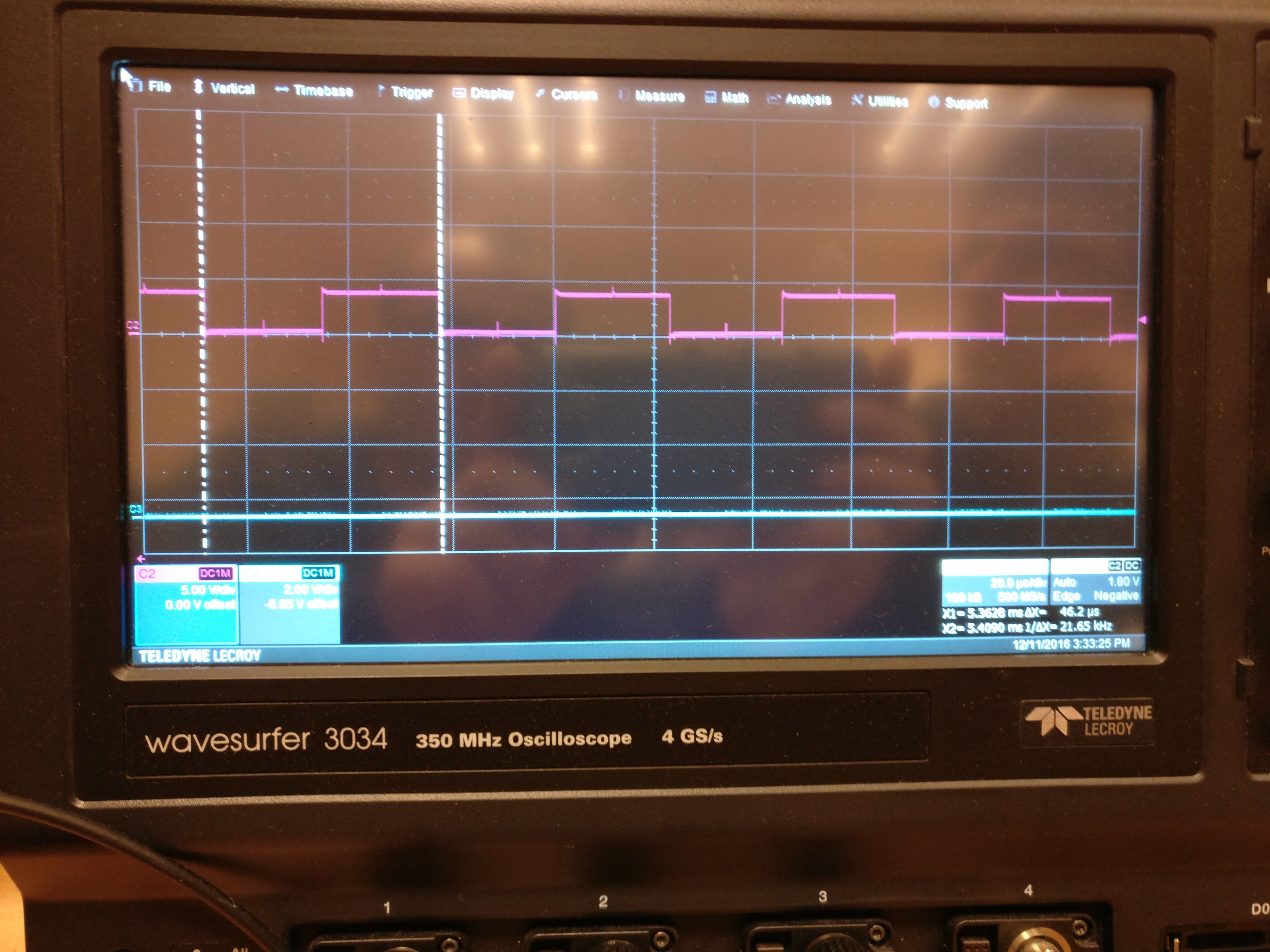
- Timing Analysis - Cursor measurements showing precise propagation delays and timing relationships
Proper PCB design addresses transmission line issues through controlled impedance traces and termination resistors. Breadboards lack these refinements, explaining why they work adequately at low frequencies but show problems as frequency increases. These limitations make breadboards excellent learning tools - they demonstrate real-world effects that students must understand for professional design work, even though the breadboard itself represents poor high-frequency design.
Crosstalk Measurements: Unintended Signal Coupling
Digital circuits ideally exhibit no interaction between separate signal paths - each wire carries its intended signal independent of neighbors. Reality differs, particularly at high frequencies where electromagnetic coupling between adjacent conductors transfers energy between supposedly isolated signals.
We measured crosstalk by driving one signal path while monitoring an adjacent, nominally quiet path. The “aggressor” signal carried our test waveform while the “victim” signal, which should have remained at steady logic level, showed small but measurable induced voltages.
Crosstalk coefficient calculation:
Kxt = Vvictim / Vaggressor ≈ 0.02 (2%)
At 44 MHz with 5Vpp aggressor signal, victim signal showed approximately 100mV induced voltage - small in absolute terms but approaching the ~400mV noise margin between valid LOW level and threshold. In dense circuitry with many parallel traces, cumulative crosstalk from multiple aggressors could cause functional failures.
Crosstalk mechanisms include both capacitive coupling (where electric field between conductors causes current flow) and inductive coupling (where magnetic field from current in one conductor induces voltage in another). At our frequencies, capacitive coupling dominated, explaining why crosstalk increased linearly with frequency and decreased with increased conductor spacing.
These measurements illustrated practical PCB design rules: maintain spacing between critical signals, route sensitive traces perpendicular to noisy traces (minimizing parallel length), use ground planes to shield between layers, and consider differential signaling for truly critical high-speed paths.
Comparative Analysis: Breadboard vs. PCB Performance
To quantify the performance degradation that breadboard construction imposed, we replicated key measurements on professionally manufactured PCBs with controlled impedance and proper ground planes. The differences proved dramatic and educational.
| Parameter | Breadboard | 2-Layer PCB | 4-Layer PCB |
|---|---|---|---|
| Characteristic Impedance | 80-150Ω (variable) | 50Ω ±10% | 50Ω ±5% |
| Propagation Delay @ 44MHz | 18.0 ns | 16.5 ns | 16.2 ns |
| Overshoot | 8% | 3% | 1% |
| Crosstalk | 2% | 0.5% | 0.1% |
| Ground Bounce | 100mV | 30mV | 10mV |
The four-layer PCB with dedicated power and ground planes showed performance approaching theoretical ideals - minimal overshoot, negligible crosstalk, and tight impedance control. The two-layer PCB performed substantially better than breadboard despite lacking dedicated planes. Even breadboard showed acceptable performance at lower frequencies, demonstrating why they remain valuable prototyping tools despite high-frequency limitations.
These comparisons taught important lessons about when breadboard prototyping suffices versus when PCB manufacturing becomes necessary. For digital circuits operating below ~10 MHz, breadboards work fine. Above 20-30 MHz, PCB benefits become significant. Above 50-100 MHz, breadboards become nearly unusable and PCBs with controlled impedance become mandatory.
Troubleshooting Techniques: Systematic Problem-Solving in Hardware
Equipment sophistication doesn’t eliminate problems - if anything, it creates opportunities for new and interesting failures. Developing systematic troubleshooting methodology proved as important as understanding measurement techniques.
Problem 1: “The Circuit Doesn’t Work” - Starting from Fundamentals
The most common problem statement from beginners: “It doesn’t work.” This vague statement provided no useful information about what specifically failed. Effective troubleshooting required transforming vague concerns into specific, testable hypotheses.
Our systematic approach started with the most basic checks:
Power Supply Verification:
- Is power supply enabled and outputting correct voltage?
- Is current draw reasonable? (Absence of current suggests open circuit; excessive current suggests short circuit)
- Do voltage measurements at IC pins match expectations?
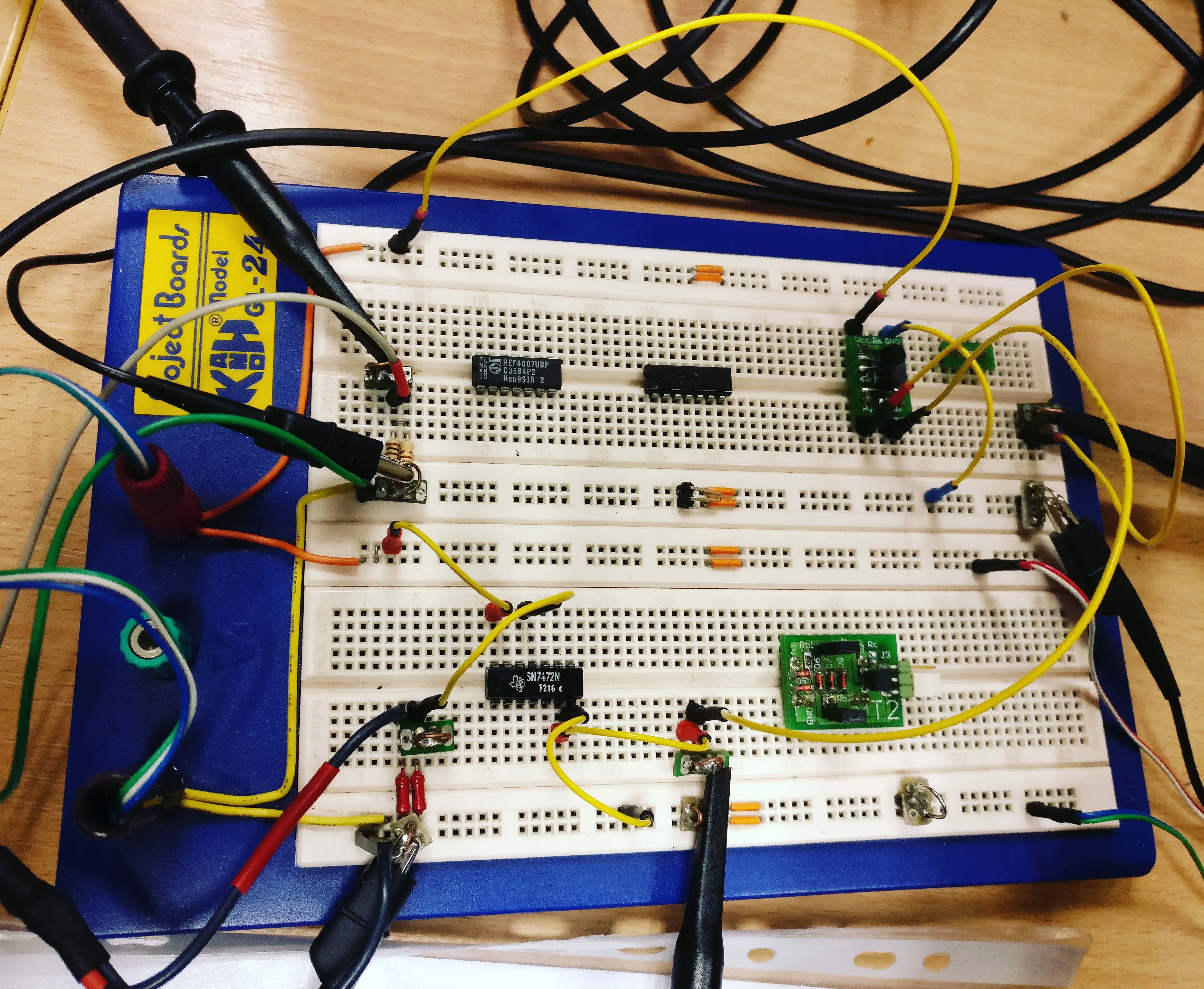
- Breadboard Close-up - Two 74LS27 ICs with visible decoupling capacitors and measurement connections
Physical Connectivity Verification:
- Are all IC pins properly inserted into breadboard?
- Do continuity checks confirm intended connections?
- Are there any unwanted short circuits?
Signal Presence Verification:
- Is signal generator actually producing output?
- Does signal reach circuit input?
- If no output exists, is the IC receiving proper signals?
This layered approach - starting from most fundamental and progressively more sophisticated - prevented common mistakes like spending hours analyzing circuit timing when the real problem was an unplugged power connection.
Problem 2: Intermittent Failures - The Most Frustrating Category
Consistent failures, while frustrating, at least provide reproducible conditions for debugging. Intermittent failures - problems that come and go seemingly randomly - present far greater challenges. These failures required different troubleshooting strategies emphasizing patterns and probabilities over simple cause-effect relationships.
Intermittent failures in our testing usually originated from physical connection problems. Breadboard contacts can become inconsistent through oxidation, damage, or simple mechanical looseness. A connection that worked initially might fail after slight vibration or temperature change. IC pins might not fully insert into breadboard holes, creating intermittent contact.
- Alternative View - Wiring routing optimized for minimal crosstalk and ground loops
Our approach to intermittent problems involved deliberate physical manipulation while monitoring circuit behavior. Gentle pressure on components, slight wire movement, temperature changes from airflow - these tests often provoked failures in reproducible ways, revealing the physical cause. Once reproducible, problems became straightforward to fix through proper connection remakes or component replacement.
Documentation proved crucial for intermittent issues. When did failures occur? What conditions preceded them? What fixed them temporarily? This record-keeping often revealed patterns invisible to immediate observation - perhaps failures occurred after 15 minutes of operation (thermal effect) or only at specific test frequencies (resonance or timing sensitivity).
Problem 3: Measurement Artifacts - Is the Problem Real or Instrument-Induced?
One particularly insidious category of “problems” involved measurement artifacts - apparent circuit misbehavior that actually represented measurement system issues rather than circuit problems. Distinguishing real circuit behavior from measurement artifacts required understanding instrument limitations and proper probe technique.
Ground loops represented a common artifact source. When oscilloscope probe ground connected to circuit at a different physical location than signal ground, a complete loop formed through earth ground via oscilloscope chassis. Current flowing through this loop (from other equipment, building ground currents, etc.) created voltage drops that appeared as noise in measurements. Fixing ground loops required connecting probe grounds to circuit ground as close as possible to measurement points, minimizing loop area.
Probe loading affected measurements at high frequencies. Oscilloscope probes present capacitive loads (typically 10-20 pF even with 10× probes) that affect circuit behavior. In high-impedance circuits, this capacitance could significantly change operation. We verified that probe loading didn’t corrupt measurements by comparing results with and without probes connected, or by using active probes with much lower input capacitance.
Aliasing represented another measurement artifact. When signal frequency exceeds half the oscilloscope’s sampling rate (the Nyquist frequency), undersampling occurs and signals appear at incorrect frequencies. Our 4 GS/s oscilloscope had 2 GHz Nyquist frequency, well above our test frequencies, but slower oscilloscopes could show aliasing artifacts that appear as real but fictitious signals.
Key Lessons: Skills That Transcend Specific Circuits
While the immediate goal involved characterizing 74LS27 gates, the deeper lessons transcended this specific component and provided transferable skills applicable throughout electronics engineering.
1. Measurement Integrity Determines Result Validity
All measurements rest on assumptions about measurement system behavior. Understanding these assumptions - probe impedance effects, oscilloscope bandwidth limitations, trigger sensitivity, ground loop potentials - separated valid measurements from meaningless noise. The mantra “garbage in, garbage out” applies equally to measurements as to software.
Before trusting any measurement, we learned to ask: Could this result represent measurement artifact? Are we measuring what we think we’re measuring? What calibrations or verifications confirm measurement system integrity? This skeptical mindset, combined with systematic verification, prevented accepting false results that could lead analysis astray.
2. Documentation Enables Collaboration and Future Reference
- Power Supply Configuration - Multiple measurements showing current draw variations across different test conditions
Complex testing generates vast amounts of data - waveform captures, numerical measurements, configuration settings, observations about circuit behavior. Without systematic documentation, this information becomes lost or confused, rendering effort partially wasted.
We maintained laboratory notebooks recording all significant tests: what we measured, how we configured equipment, what results we observed, what conclusions we drew. Equally importantly, we documented anomalies and unexpected results even when we didn’t understand them - often patterns became clear only after accumulating multiple such observations.
Screenshots captured oscilloscope displays for important measurements, providing visual records that numerical data alone couldn’t convey. These images proved invaluable when writing reports or revisiting measurements weeks later. The subtle waveform details visible in screenshots often triggered insights that numerical parameters missed.
3. Systematic Variation Reveals Relationships and Boundaries
Rather than testing at arbitrary points, systematic variation of one parameter while holding others constant revealed how parameters influenced circuit behavior. This scientific method approach - varying one factor at a time - enabled isolating cause-effect relationships and building comprehensive understanding.
Our frequency sweep (1 MHz, 10 MHz, 20 MHz, 44 MHz) showed how propagation delay remained relatively constant until approximately 30 MHz, then increased dramatically beyond that point. This revealed the frequency range where circuit operated within specifications versus where it approached limitations. Similar systematic variations of voltage, loading, and temperature built complete pictures of circuit capabilities and boundaries.
4. Theory Guides, But Measurement Reveals Reality
Theoretical calculations and datasheet parameters provided essential guidance for test planning and result interpretation. However, actual measurements often revealed subtleties that theory missed or simplified. Real components showed unit-to-unit variation, temperature dependencies, and second-order effects that idealized models ignored.
This tension between theory and measurement isn’t conflict - rather, it represents complementary approaches. Theory provides framework for understanding and predicting behavior. Measurement verifies predictions and reveals where reality diverges from idealization. Both are necessary; neither alone suffices.
5. Equipment Competence Multiplies Testing Effectiveness
Initial equipment learning curves felt steep - so many menus, so many parameters, such complex functionality. However, investment in mastering equipment operation paid enormous dividends throughout all subsequent testing. Fluency with oscilloscope operation meant quickly capturing relevant waveforms, efficiently configuring measurements, and naturally exploring circuit behavior through instrument capabilities.
This equipment competence became transferable skill. While specific instrument models differ, fundamental measurement principles remain constant. Understanding how to effectively use one professional oscilloscope provided foundation for quickly mastering others. The methodical approach to learning instruments - reading manuals, exploring menus systematically, practicing basic operations until fluent - applied to any professional test equipment.
Practical Guidance for Aspiring Hardware Engineers
Based on intensive hands-on testing experience, several recommendations emerged for anyone beginning electronics engineering or working to advance hardware debugging skills.
1. Prioritize Understanding Over Memorization
Digital electronics involves numerous parameters, specifications, and design rules. Attempting to memorize all details proves both impossible and counterproductive. Instead, focus on understanding fundamental principles from which specific details logically follow.
Understanding why decoupling capacitors matter (transient current demands create voltage fluctuations) makes their proper use natural rather than requiring memorization of “always add decoupling capacitors” as arbitrary rule. Understanding transmission line theory explains signal integrity problems at high frequencies, making seemingly mysterious ringing and reflections comprehensible as predictable physics.
This principled understanding provides flexibility that memorization cannot match. When encountering new situations, understanding enables reasoning about likely behavior and appropriate approaches, while memorization only helps when situations precisely match memorized scenarios.
2. Develop Systematic Troubleshooting Methodology
Random troubleshooting - trying various fixes hoping something works - occasionally succeeds through luck but generally wastes time and often creates additional problems. Systematic methodology - gathering information, forming hypotheses, testing specific theories, documenting results - consistently proves faster and more reliable.
This methodology becomes reflexive through practice. Initial adherence to systematic approaches feels slow and overly formal. However, repeated application builds instinctive troubleshooting patterns that engage automatically when problems arise. What began as conscious methodology becomes unconscious competence.
3. Maintain Laboratory Notebooks Consistently
Electronic lab notebooks (or physical notebooks for those preferring paper) serve multiple purposes: experimental records for current work, references for future projects facing similar challenges, and portfolios demonstrating competence to employers or collaborators.
Effective notebooks include sufficient detail for reconstruction of experiments - equipment used, configuration settings, measurement results, observations and conclusions. Screenshots, photographs, and diagrams supplement text descriptions. Most importantly, notebooks remain current through consistent use rather than sporadic after-the-fact transcription that inevitably misses important details.
4. Learn from Equipment Manuals Rather Than Avoiding Them
Professional test equipment manuals often span hundreds of pages. This intimidating length causes many users to avoid manuals, relying instead on random button pushing and hoping to stumble upon correct operation. This approach wastes opportunities for learning about sophisticated capabilities.
Better approach: treat manual reading as systematic learning rather than desperate reference during problems. Reading manuals cover-to-cover during equipment downtime (waiting for simulations, during transit time, etc.) builds comprehensive understanding of capabilities. Even seemingly irrelevant sections often prove surprisingly useful for unexpected applications.
5. Practice Estimation and Sanity-Checking
Before measuring anything, estimate expected results based on theory and experience. After measurements, compare actual results to expectations. Large discrepancies indicate either measurement problems or misunderstanding requiring investigation.
This estimation practice develops intuition about circuit behavior and catches measurement errors that might otherwise go unnoticed. When measurement shows propagation delay of 180 ns (ten times expected 18 ns), immediate recognition that something’s wrong prevents wasting time analyzing meaningless data.
Career Applications: Professional Relevance of Laboratory Experience
Hands-on laboratory experience with professional equipment provides career value extending far beyond specific technical knowledge gained during individual projects.
1. Employer Expectations Emphasize Practical Competence
Job postings for hardware engineer positions often explicitly require oscilloscope proficiency, familiarity with signal generators and power supplies, and experience with PCB debugging. These aren’t checkbox requirements - employers genuinely need engineers who can walk into laboratories and immediately begin productive work without months of equipment training.
Candidates demonstrating authentic hands-on experience stand out dramatically during technical interviews. Discussing specific troubleshooting challenges overcome, explaining measurement techniques used for particular characterization tasks, or describing equipment configuration details that only hands-on experience provides - these conversations differentiate experienced practitioners from those with only theoretical knowledge.
2. Certification Examinations Validate Practical Skills
Professional certifications in electronics (Certified Electronics Technician, various vendor-specific certifications) include practical components requiring hands-on demonstration of measurement and troubleshooting competence. Theoretical knowledge alone doesn’t suffice - candidates must show they can actually operate equipment and solve real problems.
Laboratory experience provides preparation that study guides cannot match. Fluency with equipment operation, practiced troubleshooting methodology, and experiential understanding of typical circuit behaviors enable confident performance during practical examinations.
3. Research and Development Requires Characterization Skills
R&D engineering involves creating new circuits and systems, which requires extensive testing and characterization to verify designs meet requirements. This testing demands exactly the measurement skills and equipment competence developed through laboratory work.
Engineers working on new products spend significant time in laboratories capturing waveforms, measuring performance parameters, debugging prototype problems, and characterizing environmental sensitivities. The difference between effective R&D engineers and struggling ones often lies less in design creativity than in debugging competence and measurement skill.
4. Failure Analysis Depends on Systematic Investigation
When products fail in field or production, companies need engineers who can systematically identify failure causes and recommend fixes. This failure analysis relies heavily on measurement and characterization skills - examining failed units under various conditions, comparing with functional units, isolating failure mechanisms through targeted testing.
The systematic troubleshooting methodology developed through laboratory work directly applies to failure analysis. The habit of forming testable hypotheses, gathering evidence methodically, and drawing conclusions supported by data becomes invaluable for solving real-world reliability problems.
Advanced Topics and Future Directions
Basic testing and characterization provided solid foundations, but numerous advanced topics remained for future exploration, each offering deeper insights into digital circuit behavior and measurement techniques.
1. Automated Testing and Characterization
Manual testing, while instructive, becomes impractical when comprehensive characterization requires hundreds or thousands of measurements across parameter spaces. Test automation using programming interfaces (SCPI commands over GPIB or Ethernet) enables systematic sweeps that manual operation cannot match.
Python emerged as popular language for test automation, with libraries like PyVISA providing straightforward instrument control. Scripts could automatically vary parameters, capture measurements, analyze results, and generate reports - tasks requiring days manually completing in hours automatically.
2. Mixed-Signal Analysis - Where Digital Meets Analog
Our testing focused on pure digital signals, but real systems increasingly involve mixed-signal designs combining digital and analog circuitry. Analog-to-digital converters, phase-locked loops, and switch-mode power supplies all require analysis techniques spanning both domains.
Mixed-signal measurement introduces additional complexities: understanding quantization noise, analyzing clock jitter effects on conversion accuracy, characterizing switching noise coupled into analog circuits. These challenges require combining digital measurement skills with analog circuit knowledge.
3. High-Speed Serial Links and Eye Diagrams
Modern digital systems increasingly use high-speed serial links (USB, PCIe, SATA) rather than parallel buses, operating at gigabit/second rates where our tens-of-MHz testing represented slow operation. Characterizing these links requires new techniques, particularly eye diagram analysis.
Eye diagrams overlay many signal transitions to statistically characterize signal quality - showing not just typical behavior but worst-case variations. Understanding eye diagram interpretation, mask testing, and jitter decomposition represents critical skills for modern digital system validation.
4. Electromagnetic Compatibility (EMC) Testing
Our testing touched on electromagnetic interference through crosstalk measurements, but comprehensive EMC characterization requires specialized equipment and techniques. Spectrum analyzers, near-field probes, and anechoic chambers enable quantifying emissions and susceptibility to interference.
EMC represents crucial concern for commercial products, which must pass regulatory compliance testing (FCC in US, CE in Europe) before sale. Understanding EMC testing principles and design techniques for achieving compliance becomes essential for product development engineers.
5. Formal Verification Through Simulation
While we performed empirical testing on physical hardware, complementary approach involves SPICE simulation for circuit analysis before hardware construction. SPICE (Simulation Program with Integrated Circuit Emphasis) enables predicting circuit behavior, optimizing designs, and verifying performance before committing to hardware builds.
Learning to effectively use SPICE requires understanding both circuit theory (to create accurate models) and simulation tools (to configure appropriate analyses and interpret results). Combined empirical testing and simulation provides powerful workflow for efficient circuit development.
Conclusion: Transformation Through Hands-On Mastery
This comprehensive testing experience with 74LS27 logic gates transformed abstract digital electronics concepts into concrete, experiential knowledge. The journey from initial equipment setup through systematic characterization to advanced analysis represented fundamental skill development that will serve throughout entire engineering career.
The photographs documenting our work show breadboards with integrated circuits, oscilloscope screens displaying waveforms, and professional test equipment configurations. What they cannot capture is the progression from initial uncertainty (“How do I even use this oscilloscope?”) through growing competence (“I can configure basic measurements”) to eventual mastery (“I understand what these signals mean and how to extract useful information from complex waveforms”).
For anyone studying electronics or contemplating hardware engineering career, I cannot overemphasize the value of extensive hands-on laboratory experience. Reading textbooks provides essential theoretical foundations. Watching demonstration videos offers helpful examples. But nothing replaces direct experience working with actual circuits using professional equipment, encountering real problems that textbooks never mentioned, developing troubleshooting instincts through repeated practice, and building intuitive understanding of circuit behavior that only comes from seeing hundreds of waveforms under various conditions.
The path from “I’ve read about digital circuits” to “I can design, build, and debug real digital systems” runs directly through laboratories equipped with professional test equipment. It’s challenging work that occasionally frustrates, but the skills developed prove invaluable throughout entire careers. Every expert hardware engineer remembers their early laboratory experiences - those formative sessions where theoretical knowledge transformed into practical competence.
To anyone beginning their hardware journey: Embrace every laboratory opportunity. Don’t just follow lab instructions mechanically - understand why each step matters. Ask questions fearlessly, even when they seem basic - no question is too simple if it deepens your understanding. Experiment boldly with configurations in safe laboratory environments - break things deliberately to learn how to fix them. Document your work meticulously - future you will thank present you for those notes. Most importantly, persist through frustrations - every struggle builds skills and every mistake teaches lessons.
Remember that every hardware expert began exactly where you are now - as a beginner uncertain about basic concepts, making common mistakes, gradually building competence through practice and persistence. The difference between beginners and experts isn’t innate talent - it’s accumulated experience gained through dedicated laboratory work over time.
The skills developed through these testing sessions form foundations supporting entire hardware engineering careers. Whether you pursue R&D designing new circuits, production supporting manufacturing operations, field applications supporting customer deployments, or research exploring fundamental device physics, the core competencies of systematic measurement, equipment proficiency, and analytical troubleshooting remain relevant and valuable.
Digital electronics offers fascinating, challenging, and rewarding careers for those willing to invest in developing practical skills. These laboratory sessions represent just the beginning of that journey - an essential first step toward expertise that will serve you throughout your professional life.
This site runs on coffee and good intentions. Help keep it running?
References:
- Texas Instruments. (2004). 74LS27 Triple 3-Input Positive-NOR Gates Datasheet. Texas Instruments.
- Teledyne LeCroy. (2023). WaveSurfer 3000 Series Oscilloscope User Manual. Teledyne LeCroy Corporation.
- Rohde & Schwarz. (2022). HMP Series Power Supply Operating Manual. Rohde & Schwarz GmbH & Co KG.
- Johnson, H. & Graham, M. (2003). High-Speed Digital Design: A Handbook of Black Magic. Prentice Hall.
- Horowitz, P. & Hill, W. (2015). The Art of Electronics (3rd ed.). Cambridge University Press.
- Signal Integrity Fundamentals - Educational resource for high-speed design.
- Bogatin, E. (2009). Signal and Power Integrity - Simplified (2nd ed.). Prentice Hall.
- Williams, T. (2017). EMC for Product Designers (5th ed.). Newnes.